Note 3 Circuit Diagram
Galaxy note3 n9005 smart phone repair reference schematic pcb board Samsung galaxy note10+ schematics Boss ge-10 service note p.3 circuit diagram planer, electrical wiring
[View 34+] Samsung Note 4 Schematic Diagram Pdf
[view 34+] samsung note 4 schematic diagram pdf Mi note 5 circuit diagram Samsung note sm layout pcb n950u
Oppo a5s schematic schematics mobile1tech
Schematics note10 n970fVoltage over under cut power circuits diagrams ac circuit electronic dc relay supply schematic load low schematics electrical electronics connect Solved note the diagram below, which shows a circuit createdSamsung galaxy note 9 sm-n960f circuit diagram service manual schematic.
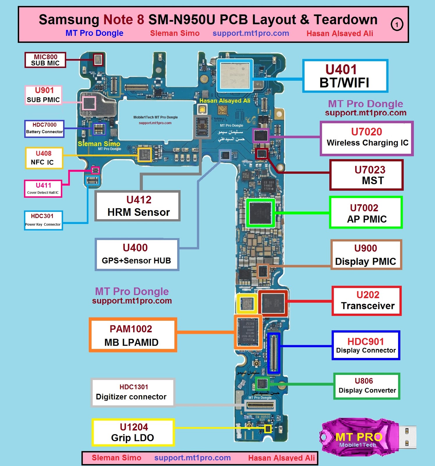
Samsung galaxy note 3 sm-n900 lcd dispaly not working solutionSamsung galaxy note20 ultra sm-n986u schematics Samsung note 8 sm-n950u pcb layout &teardownSamsung note 8 sm-n950u pcb layout &teardown.

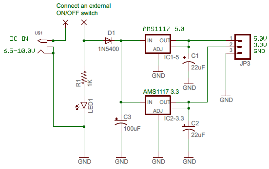
Ams1117 circuit regulator supply power dual 3v voltage ams diagram board multi 0v note ldo electronic components fans crazy 1a
Redmi note pro schematic qualcomm jmh xiaomi diagrams[view 25+] samsung galaxy note 4 schematic diagram Synapse circuit technology review: the synapse circuit samsung galaxyGalaxy n900 schematic circuit.
Samsung galaxy note 3 n900a touch screen solution waysNote galaxy schematic diagram manual pcb board repair phone maintenance reference smart a7 note3 edge note4 electronic n9005 mouse zoom Schematic samsung galaxy note 8 gt-n5100Samsung galaxy note10+ sm-n975f schematic and pcb layout (*.pdf.
![[View 39+] Samsung Note 4 Schematic Diagram](https://i.pinimg.com/originals/d3/70/f1/d370f1b93da5ea97a13b682f2266a2ec.png)
Note the diagram below which shows a circuit created with a battery and
Samsung galaxy note 3 circuit diagram : r/mobilerepairSamsung galaxy note 3 neo sm-n7505 schematics Patrice benoit art: [45+] note 4 schematic diagramRedmi note 3 pro (qualcomm) schematic & layout diagrams.
Samsung note 4 n910f motherboard schematic diagram service ways ic[view 39+] samsung note 4 schematic diagram Celulares esquemas eletricosCircuit diagram note shows below which bulbs battery created ohm three law.

Samsung note 8 sm-n950u pcb layout &teardown
Samsung galaxy note 3 neo sm-n7505 schematicsNote touch samsung n900a screen solution galaxy ways [view 34+] samsung note 4 schematic diagram pdfSchematics samsung note 9 sm-n960n (direct link).
Samsung note n900 galaxy sm dead support solution haldwani unofficial zone welcome siteSamsung galaxy note 3 sm-n900 schematics Schematics note10Samsung galaxy note10 sm-n970f schematics.

Samsung note pcb sm n950u layout teardown
N900 schematics đồ mạch tiết sơSamsung galaxy note10 lite / sm-n770f schematics N770f schematics note10Note samsung galaxy colors synapse circuit review smartphones phone wallpapers core note3.
Figure 3. circuit diagram [2] : solar powered mobile power bank systemsRedmi schematic Diagram figure solar power circuit figures previous index next bankSamsung galaxy note 3 sm-n900 dead solution ~ mobile support.
Over / under voltage cut-out
Mi note xiaomi diagram circuit max2 wiring[view 39+] samsung note 4 schematic diagram Galaxy schematic circuitElectronic components crazy fans: january 2013.
Samsung sm noteSchematics note10 n975u Note samsung galaxy diagram circuit ic n9005 n900 disassembly numberCircuit note below physical diagram which diagrams represent shows solved expert answer arrangement apply shown select above may.

![[View 39+] Samsung Note 4 Schematic Diagram](https://i2.wp.com/phonelumi.com/wp-content/uploads/2019/10/schematics-samsung-galaxy-note10.jpg)
![[View 34+] Samsung Note 4 Schematic Diagram Pdf](https://i.ytimg.com/vi/PHrXeOStnvU/mqdefault.jpg)